Sloshing Electrons and Crossing Oceans

On December 12, 1901, Guglielmo Marconi sent the first radio transmission across the Atlantic Ocean. This historic moment marked the dawn of a new era of wireless communication. The transmitter he used was designed by Sir John Ambrose Fleming. This demonstration proved that radio waves could travel beyond the line of sight, bending with the curvature of the Earth. Imagine how Fleming must have felt, knowing the transmitter he built had accomplished this remarkable feat. Even after more than 120 years, it still seems awe-inspiring. What better way to relive that excitement than by building your own transmitter and sending a signal across the vast open ocean?

Designing a Transmitter

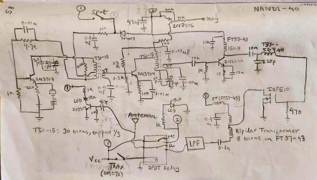
I began working on a CW (Continuous Wave) transmitter inspired by the book “Crystal Sets to Sideband” written by my dear friend Frank Harris (K0IYE). In general, CW transmitters are simple to build and understand. You slosh electrons back and forth at just the right frequency, and you will generate a form of invisible light that can travel thousands of kilometers. I’m referring to electromagnetic waves, of course! CW doesn’t transmit voice; it is just an unmodulated carrier wave. Communication happens through Morse code.

Oil lamps for an authentic early 1900s feel
Oil lamps for an early 20th-century vibe

I built the oscillator and buffer amp exactly as described in Frank’s book. The oscillator is a Butler-type oscillator, which is a rather unusual choice. Most circuits use a Hartley or Colpitts oscillator, but Frank mentioned that the Butler oscillator has little start-up drift.

Tuning the buffer amp

The buffer amp bumps the output of the oscillator to about 50 mW and adds a layer of separation between the oscillator and the subsequent stages. This helps keep the load on the oscillator as light as possible.

I didn’t have the same transistor Frank was using in the final PA (Power Amp), so I took it as an opportunity to design the rest of the circuit on my own. I decided to use the ubiquitous IRF510 MOSFET, which I had in abundance. After experimenting with the IRF510, I realized I would need at least 200-300 mW of drive to generate 5W+ of RF power, which is what I was aiming for. I realized my puny buffer amp didn’t have the juice to do it.

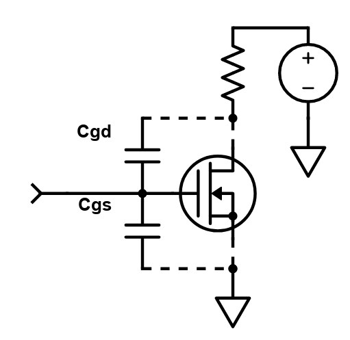
But aren’t MOSFETs voltage-driven devices with sky-high input impedance? Yes, that’s true when you look at them from a DC perspective. But the high impedance goes out the window once you start dealing with high-frequency AC signals. The gate is essentially like a capacitor. Depending on the frequency (and other factors which I’ll discuss), its impedance changes. So, I had to design another “driver” amp stage to drive the IRF510.

I experimented with several types of driver amp circuits. Some of the ones that I tried to design on my own didn’t work so well. I finally settled on a design I found in the book “Experimental Methods in RF Design” by Wes Hayward et al. It produces about 300-400 mW with an efficiency of about 70% (typical for Class C). This is more than enough to satisfy the IRF510.

What makes the IRF510 interesting is that it was made by International Rectifier in the 1970s for the automotive industry. It was used to replace clunky electromechanical relays being used in blinkers and dimmers. Who would’ve guessed that decades later, it would become a favorite among amateur radio builders, operating at frequencies far beyond what it was originally designed for!

The Full Circuit

Nandi-40 circuit

The Gate Capacitance Paradox

Connecting the driver stage to the power amp was a challenge. In RF circuits, matching one stage to another often involves some sort of matching network. I’ve talked about this in my blog post about impedance matching and archery.

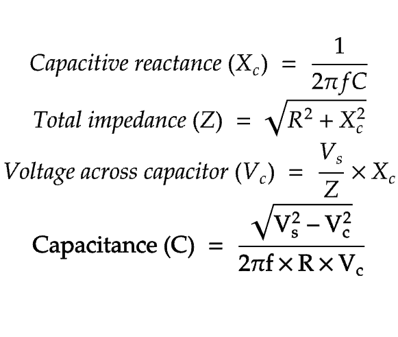
I tried to be methodical about designing the matching network. I started off by determining the output impedance of the driver stage by loading it with different resistors and recording the voltages. Here is the formula:

This formula is useful when driving the amp without a load is undesired. However, if the open circuit voltage can be measured, this formula could be used:

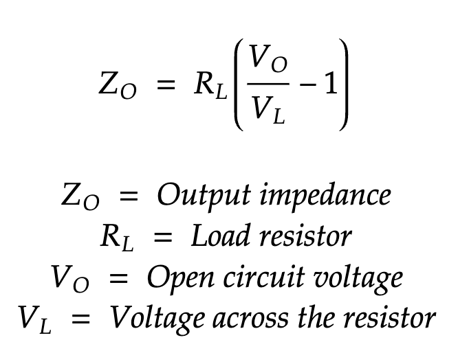
These equations are not magical; they could easily be derived using Ohm’s law and the basic voltage divider equation. I determined the input impedance of the IRF510 (about 220 ohms) by using a signal generator and measuring the voltage across the gate with an oscilloscope. The output impedance of the signal generator and the input impedance of the IRF510 form a voltage divider. The voltage divider formula can be used to determine the unknown input impedance.

I discovered that the input impedance of a MOSFET isn’t fixed. It is dynamic and changes with the drive voltage. If the drive voltage is below the IRF510’s gate threshold voltage Vgs(th), its impedance appears quite high. Once the voltage goes above the threshold, it starts dropping. After some speculation, I came to the conclusion that this is the result of the Miller effect. I’ve encountered this phenomenon in another experiment in the past.

Miller Effect

“In electronics, the Miller effect accounts for the increase in the equivalent input capacitance of an inverting voltage amplifier due to amplification of the effect of capacitance between the input and output terminals.

So, when the capacitance increases, the capacitive reactance decreases, since they are inversely related. This reduces the effective impedance of the gate. Well, I guess that explains the mystery.

I initially tried designing an LC L-match to match the output of the driver to the input of the MOSFET. But despite careful calculations, the PA didn’t perform well. I also experimented with transformer coupling using a 10:3 turns ratio, but that approach didn’t yield good results either.

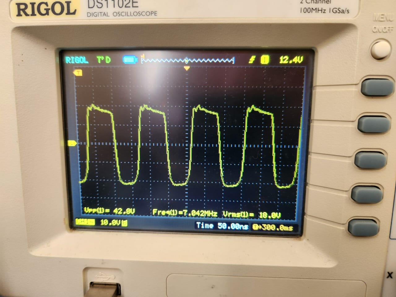
Eventually, I settled on an L-match configuration with the shunt element placed on the driver side, which has lower impedance than the MOSFET’s input. This goes against convention, as the shunt element is typically placed on the higher impedance side. Yet, to my surprise, this unconventional setup worked significantly better. I think this is because this LC network forms a low-pass filter, which removes frequencies above a certain cut-off frequency. In my case, the values I’ve used would have a cut-off near 7 MHz. However, this filter could be tweaked to improve performance. It seems these values are not too critical. If you reduce the cut-off frequency, you would have a lower voltage at the MOSFET’s gate.

I’m not aiming for maximum power transfer with this matching network. Instead, I’m using a low-pass filter to ensure sufficient voltage swing—around 10V at the MOSFET gate—to drive it into saturation without exceeding its ±20V maximum gate rating.

The Gate Resistor’s Little Secret

I have a 470-ohm resistor connected to the gate of the MOSFET to provide a ground reference. I initially used a large 1 megaohm resistor to reduce resistive loading on the driver stage, but the transmitter performed poorly.

After some experimentation, I came to suspect that this resistor plays another important, and less obvious role: discharging the gate-to-source capacitance (Cgs) between RF pulses. This helps ensure the MOSFET remains off during the portions of the cycle outside its conduction angle. At 7 MHz, the period is just 142 nanoseconds. If the resistor is too large, Cgs doesn’t fully discharge between pulses. After experimentation, I settled on a 470-ohm resistor. A 1K resistor also worked well, but going much higher started to degrade the results.

Transmit, Receive, and Keying

The transmitter has a transmit/receive (Tx/Rx) switch. While it doesn’t have a built-in receiver, an external receiver can be connected and used alongside it. For Tx/Rx switching, I use a small DPDT relay. In receive mode, the relay completely cuts power to the transmitter to avoid interference.

I also added a “spot” button that can be pressed while in receive mode. This powers up just the oscillator, allowing me to hear its tone on the receiver. This lets me check if I’m in tune with another operator’s CW signal, kind of like tuning a guitar to match pitch.

In transmit mode, the oscillator runs continuously. Pressing the key activates the buffer amplifier stage using a PNP transistor. Once enabled, the buffer amp passes the oscillator signal to the subsequent stages. This approach ensures that the small PNP transistor isn’t burdened with the high current demands of the driver and power amplifier. Instead, it simply triggers the buffer amp.

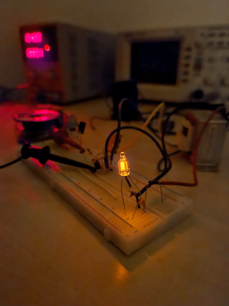
I also added two LEDs for visual feedback. One LED indicates when the transmitter is in Tx mode. The second LED lights up when the transmitter is keyed, specifically, when an RF signal is being fed into the antenna. It helps verify that everything is working as expected. If this LED doesn’t light up, it means no RF is reaching the antenna, and something’s wrong. To minimize the current draw from the RF path, I used a transistor to drive this LED.

Cleaning the Output

Unlike Marconi, we can’t use a noisy spark transmitter on the air. The output from the PA was noisy and full of harmonics. I used a low-pass filter (LPF) to clean it up.

Before filtering
After filtering

I tried designing a 5-element filter on my own. While it worked, its filtering wasn’t as strong as I would have liked. I did learn about filter design and Smith charts in the process.

In the end, I settled on a 7-element 40m LPF kit from QRPLabs that was cheaper than buying the components individually. It worked really well.

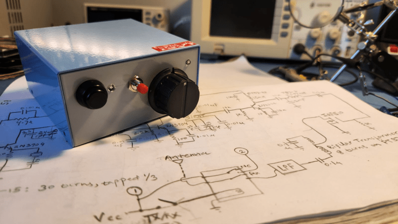
The Finished Transmitter

I named the finished transmitter “Nandi-40” because I live near Nandi Hills, and “40” refers to the 40m wavelength of the radio waves it produces. With a fully charged 12 V battery, it puts out about 10-12 watts of RF energy. With a 9V supply, it delivers about 4 watts. It definitely exceeded my design goals. Now it is time to see if it can cross the ocean like Fleming’s transmitter!

Transoceanic Transmission

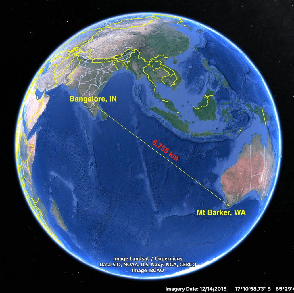
I waited for good propagation on the 40-meter band. As the sun dipped below the horizon and conditions aligned, I tuned in to a web-SDR receiver in Mt. Barker, Australia. These Australian receivers have a very low noise floor. If the Nandi-40’s automotive MOSFET was indeed stirring the ether, there was a good chance I might hear it.

I keyed the letter “S” in Morse code, three simple dots, just like Marconi did. And to my amazement, those three little blips rose above the noise floor in Australia, nearly 6,700 kilometers away!

Sure, long-distance communication is nothing new in the world of amateur radio. But there’s something uniquely satisfying and almost magical about doing it with a transmitter you built yourself.

The transoceanic transmission

Faraday’s Green Flame

I decided to step outside my usual comfort zone of electronics and explore the fascinating world of chemistry. My interest sparked after reading Michael Faraday’s book, The Chemical History of a Candle. One of the experiments in the book describes Faraday creating a green flame. A green flame seemed fascinating. I decided to replicate the experiment by synthesizing copper chloride. You can watch my video to see how it turned out!


I created my own spectroscope using a broken CD and a cardboard tube to study the spectral patterns of different light sources.

The Quantum Tunneling Transmitter

This has to be one of the most bizarre projects I have worked on. It is a transmitter that works without any transistors or tubes. It utilizes a strange phenomenon known as quantum tunneling. Quantum tunneling is a phenomenon wherein a particle can disappear from one side of a barrier and reappear on the other side even if it doesn’t have sufficient energy to surmount the barrier. It seems as if the particle “tunnels through” the barrier, hence the name. Quantum tunneling is a consequence of the wave nature of matter. It is nothing less than magic.

The first semiconductor devices to utilize this phenomenon were invented in the 1950s and were called tunnel diodes. These devices exhibit negative resistance, which means that the current through the semiconductor becomes inversely proportional to the voltage across it. This only happens at certain voltages. Below and above that negative resistance region, the tunnel diode exhibits a normal current-voltage relationship.

Current-voltage characteristics of tunnel diode vs conventional diode (from: RCAs Tunnel Diode Manual)

This negative resistance anomaly allows tunnel diodes to be used in very high-frequency oscillators. Tunnel diodes are an exotic breed of semiconductor devices. Commercially made ones are rare and expensive. However, recently, a genius inventor by the name of Nyle Steiner discovered an easily made substitute. He found out that he could make tunnel diodes at home by heating galvanized sheet metal!

Anyone with a propane torch and a few scraps of galvanized sheet metal laying around can easily make a negative resistance device. With this device, it is possible to make very simple RF oscillators, audio oscillators and even amplifier circuits. It is almost like making your own transistor.

Nyle Steiner

Mr. Steiner has some of the most interesting experiments I have seen, so do check out his website – http://www.sparkbangbuzz.com/.

I recreated the experiment by heating a zinc metal plate with a torch. The back side of the zinc plate (opposite from the flame) had several active spots. These black spots are where you are most likely to find negative resistance. I used a “cat whisker” style detector similar to the ones used in crystal radios to probe the zinc plate. For the “whisker”, I used #30 AWG copper wire.

Close-up of “cat whisker” tunnel diode
Zinc negative resistance oscillator

I’ve used a 4 MHz crystal to set the frequency of the oscillator. The 10K pot is used to adjust the biasing. The 1K resistor was initially added to reduce short-circuit current when the pot is at its lowest setting. This resistor may no longer be necessary after I added a 1K resistor in the keying circuit (which consists of a CW straight-key, 1K resistor, and an electrolytic capacitor). The keying circuit was a later addition, so I forgot to remove the 1K from the biasing circuit. The resistor and electrolytic capacitor on the keying circuit serve an important purpose. They smooth out the keying. The charge on the capacitor prevents the voltage on the cat-whisker from changing abruptly. For some reason, the homemade tunnel diode doesn’t like abrupt keying. Without the smoothing circuit, there are many cat-whisker settings that stop working after opening and closing the key. These oscillators are quite fussy.

Adjusting the cat-whisker is time-consuming task. Be prepared to spend several minutes trying to find good spots. The easiest way to know if the circuit is oscillating is by using a radio or an oscilloscope. I tuned my Icom transceiver to the frequency of the crystal (4 MHz) and kept it nearby in CW mode. You will hear clicks and beeps as you slide the cat-whisker. If you don’t, adjust the biasing. Finding a stable spot can take a while, but once you’ve found it, it can last for a long time if you don’t disturb it. In my experiments, I was able to use a spot for an entire day. It would have lasted longer if I hadn’t disturbed it.

Output of negative resistance oscillator

Here is the “quantum tunneling transmitter” in action:

I will try injecting an AM audio signal into the oscillator. I’m sure that would also work. If only the professor on Gilligan’s Island knew about it!

Some Observations on MOSFETs

I have been working on a QRP CW transmitter which I’ve described in an earlier post. The output from the buffer amplifier stage is about 50 mW. My goal is to reach about 5 watts of power. To do so, I plan to use the ubiquitous IRF510 transistor to boost power levels. The IRF510 MOSFET is a type of field-effect transistor. It was developed in the 1970s by a semiconductor manufacturing company – International Rectifier. It was originally intended to be used in the automotive industry for turn-signal blinkers and headlight dimmers to replace clunky electromechanical switches and relays. It still continues to be quite popular (and cheap). It has found its way into the hands of amateur radio experimenters who use it at frequencies way beyond what this humble transistor was intended for!

The final power amplifier in my transmitter would be a class-C amplifier using the IRF510. Before connecting the IRF510 to my circuit, I decided to investigate its input characteristics. This would help me to decide how to drive it and meet my design goals. MOSFETs typically have a very high input impedance in DC circuits since the gate is electrically insulated. However, in AC circuits, things are a little more complicated.

MOSFET basics

The IRF510 is an N-channel enhancement mode MOSFET. A MOSFET consists of an insulated gate, the voltage of which determines the conductivity of the device. The ability to regulate the flow of electricity with the amount of applied voltage can be used for amplifying or switching electrical signals.

A thin oxide layer insulates the gate from the rest of the transistor body. When a positive voltage is applied at the gate, positively charged holes are pushed away from the gate-insulator/semiconductor interface creating a depletion layer. The depletion layer is filled with negative charge carriers. With sufficient gate voltage, the accumulation of electrons forms a conducting path between the source and drain terminals, enabling current flow. The width and conductivity of the channel can be modulated by the voltage applied to the gate. The threshold voltage, commonly abbreviated as Vth of a field-effect transistor (FET) is the minimum gate-to-source voltage (Vgs) that is needed to create a conducting path between the source and drain terminals.

Gate capacitance

The gate of the MOSFET is electrically insulated because of the oxide layer, which gives it a high input impedance. When a DC voltage is applied to the gate, no current flows through the gate. The insulating oxide layer is sandwiched between two conductive layers. However, whenever two conductors are separated by an insulating layer, there will be some capacitance. Oftentimes this parasitic capacitance is an unwanted side effect. In the case of MOSFETs, this implies that the gate won’t appear high impedance to an AC input signal since capacitors allow AC signals.

The transistor datasheet should mention the gate capacitance. For the IRF510, the datasheet states a gate capacitance of about 180 pF. This could also be measured in several ways.

Observing the depletion layer

We can measure the capacitance between the gate and source pins using an LCR meter. When measuring the capacitance, I noticed that this capacitance decreases when voltage is applied to the drain and source pins (Vds). I guess this is because of the formation of the depletion layer. As the depletion layer widens, the capacitance decreases.

Gate capacitance (Vds = 0)
Gate capacitance (Vds = 10V)

Analysis with a signal generator and oscilloscope

Gate capacitance could also be determined using AC analysis with a signal generator and oscilloscope. This method involves some math.

We connect a known resistor (R) in series with the gate to create a series RC circuit. Vs is the peak-to-peak from the signal generator, and Vc is the peak-to-peak voltage measured across the capacitor on the scope. The first equation is the formula for capacitive reactance since a capacitor behaves as a frequency-dependent resistor in an AC circuit. The second equation calculates the total impedance by taking the Pythagorean sum of R and Xc. You can read more about impedance in RLC circuits here. The third equation is Ohm’s law: V = IR. The voltage across the capacitor (Vc) is equal to the total current (Vs / Z) multiplied by the reactance of the capacitor (Xc). I derived the formula for capacitance from the first three equations. If you use this method, make sure you consider the output impedance of the signal generator in your calculations.

An interesting phenomenon

While trying to determine the gate capacitance, I tried measuring the RC time constant by charging the gate capacitor through a known resistor. The RC time constant equals R x C (R is in ohms, C is in farads). The time constant is the time it takes for a capacitor to acquire 63.2% of the difference between its initial voltage charge and the voltage applied to it. When I tried measuring this, I noticed something unusual.

Miller effect

The graph doesn’t look like a typical capacitor charge graph. There is a region where it plateaus for a while before it resumes charging again.

This effect was first discovered in the 1920s by John Milton Miler when working with triode vacuum tube amplifiers. The parasitic capacitance between the grid and anode affected the performance of the triode amplifier. This effect is called “Miller effect”. According to Wikipedia:

“In electronics, the Miller effect accounts for the increase in the equivalent input capacitance of an inverting voltage amplifier due to amplification of the effect of capacitance between the input and output terminals.

Later on, we invented solid-state transistors that replaced vacuum tubes, but the Miller effect didn’t go away. There’s no getting around physics! To observe the Miller effect on a scope, I added a 10K resistor in series with the MOSFET’s gate. This resistor slows the charging time of the parasitic capacitors and allows us to see the Miller effect in all its glory.

Parasitic capacitance at the gate

In a MOSFET, there is parasitic capacitance between the gate and source (Cgs) and between the gate and drain (Cgd). There is also parasitic capacitance between the drain and the source, but we will ignore that for now. Initially, when there is no voltage at the gate, the Cgs capacitor is at 0V. The Cgd capacitor is charged to the supply voltage since the voltage at the drain is whatever the supply voltage is.

When the gate voltage rises, the Cgs capacitor charges until the MOSFET’s Vth threshold is reached. This is the voltage at which a channel is formed between the drain and the source. As the MOSFET switches on, the drain voltage drops, and eventually approaches the source voltage. When it drops, the Cgd capacitor sucks in current from the gate, preventing its voltage from rising. This is why we see the plateau in the graph. When the drain voltage settles, and the Cgd capacitor is fully saturated, the gate voltage continues rising.

How do we counter this effect? Of course, the higher the input drive current, the quicker it would pass the Miller plateau. There are other more complicated techniques to counter this effect. I don’t fully understand them yet.

The reality is that I can’t just drive the IRF510 with the 50 mW output from the buffer amplifier and expect 5 watts of output power. According to “Handiman’s guide to MOSFET amplifiers”, the input impedance is about 130 ohms at 7 MHz (40-meter band). To provide an 8 Vpp at that impedance, we’d require about a half-watt of drive. I would have to add another amplifier stage to drive the IRF510.