A few months ago, I visited Jantar Mantar in Jaipur, where I was fascinated by all the giant sundials. After I got home, I went down a rabbit hole of sundials and astronomy. For a sundial to work properly, it has to be aligned with true north and adjusted for your latitude. This allows the sundial to compensate for the monthly variations in the Sun’s apparent position in the sky (its declination).
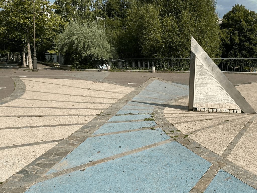
Typically, a sundial indicates the local solar time. However, a sundial could potentially also tell you the approximate date and month. This felt like a fun little problem to work on. I soon realized this wasn’t a unique idea and had already been done. The Cadran solaire Papillon in Paris is a sundial that is based on this idea:
To understand how this type of sundial would work, a basic understanding of astronomy is necessary. The Sun’s declination changes throughout the year as it moves between the Tropic of Cancer and the Tropic of Capricorn. As the Sun’s position changes, so do the direction and length of shadows that it casts. In a sundial, the object that casts a shadow is called a gnomon. Because both the direction and length of a shadow depend on the Sun’s declination, the shadow already carries information about the time of year. The paths traced by shadows on the ground are a direct record of the Sun’s journey across the sky! It’s remarkable how much we can learn about planetary motion simply by observing something as ordinary as a shadow.
I came across this website that has printable sundials that show the shadow path for different months. This seems very similar to the one in Paris. However, I couldn’t figure out how the shadow paths were determined. Of course, we could map the paths for an entire year, but that would be a lot of work. Moreover, it wouldn’t work if I were to move to another location.
I soon realized that solving this problem would require an understanding of both astronomy and mathematics. On the astronomy side, it meant understanding how the Sun’s position changes throughout the year, as well as concepts like the celestial equator and celestial coordinate systems. The mathematics, however, is more demanding. I hadn’t really used higher mathematics since college, apart from occasional applications in electronics projects. I had to step back and revisit vectors, trigonometry, and linear algebra. I actually enjoyed getting an opportunity to study mathematics again after many years.
The first step to mapping the Sun’s journey through the sky using shadows is identifying the parameters that influence shadows:
- Time of day: Shadows are longest in the early morning and late evening, and shortest around solar noon.
- Latitude: The farther we are from the equator, the longer shadows tend to be for the same solar position.
- Solar declination: The Sun’s apparent position shifts throughout the year, causing seasonal changes in shadow length and direction.
- Gnomon length: The height of the object casting the shadow directly affects the shadow’s length.
Our task, then, is to develop equations that relate these parameters and allow us to map the Sun’s apparent journey across the sky using the shadows it produces.
Two Ways to See The Sky
I approached this problem by representing the Sun as a vector, which lets us predict how it would interact with a gnomon to cast a shadow. To describe the position of the Sun as a vector, we have to first define how we “look” at space. By looking at space, I mean the coordinate basis vectors that define the space in which the Earth and Sun exist. One way is to describe this space from Earth’s perspective; the other is to describe it from our (local) perspective. We use the “topocentric equatorial coordinate system” for Earth’s perspective as it is anchored to the geometry of the Earth itself. To describe space from our perspective, we use the ENU (East-North-Up) coordinate system. The topocentric equatorial frame essentially tells us how the time of day and solar declination influence the solar vector. The ENU frame tells us how latitude influences this vector.
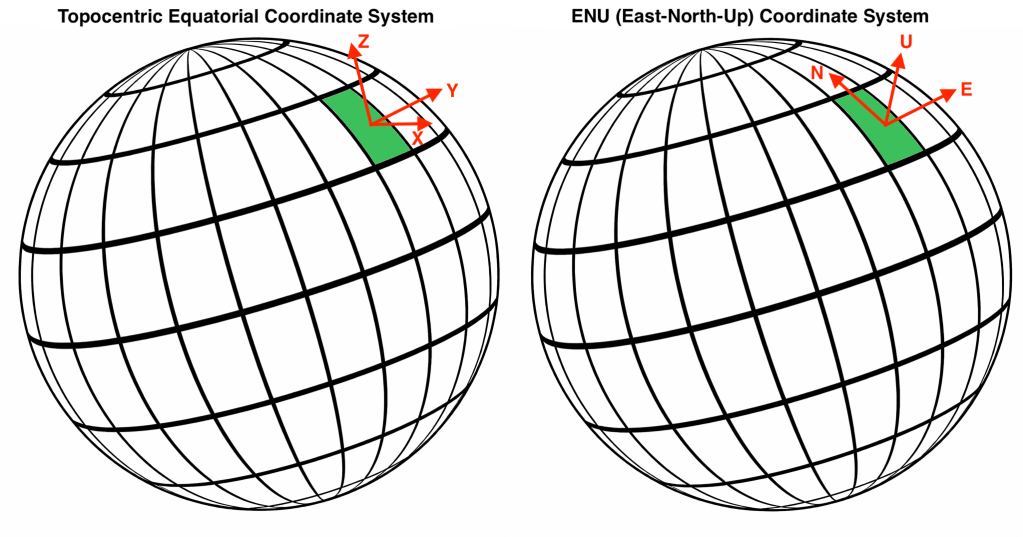
So, why use two coordinate systems to describe the same vector? In the topocentric equatorial frame, it is easy to describe the motion of the Sun from Earth’s perspective. The Sun’s path is simply governed by Earth’s rotation. However, this frame does not tell us how latitude influences the vector. This is answered in the ENU frame. We experience the sky through the ENU frame, which is tied directly to the ground beneath our feet. Where we stand on Earth determines how the sky appears to move above us.
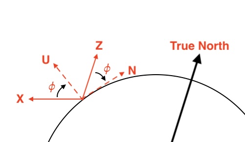
In the topocentric frame, the axes are:
- Z-axis → up along Earth’s axis toward the celestial north pole (parallel to Earth’s axis).
- X-axis → lies in the celestial equatorial plane, pointing toward the local meridian.
- Y-axis → points East.
In the ENU frame:
- E-axis → East (same as the Y-axis in the topocentric frame).
- N-axis → points towards the north pole (but it is not parallel to Earth’s axis).
- U-axis → points straight up (zenith).
Understanding the Language of Shadows with Mathematics
I used to dislike mathematics when I was in school, and I wasn’t particularly good at it either. But I never let school get in the way of my education. I started enjoying mathematics later in life, when I could study at my own pace without the pressure of exams. I realized it can be quite enjoyable if you don’t let school ruin it for you. And if you’re really lucky, you’ll come across a teacher who sparks your interest in a subject. For me, it was Dr. David Brown at Utah State University who introduced me to the beauty of linear algebra.
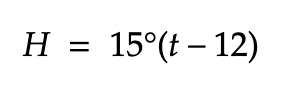
To understand the Sun’s motion, let’s start with the topocentric equatorial frame and define the Sun’s rotation as seen from Earth’s perspective. This will enable us to describe how the solar vector changes in relation to the Sun’s declination and hour angle. The hour angle is the angle of the sun from our local meridian. Since a day is 24 hours long, the Sun takes 24 hours to cover 360 degrees. So, every hour, it covers 15 degrees. The formula for the hour angle (H) is:
Throughout the day, the Sun appears to rotate about the Z-axis in the topocentric equatorial frame. If you think about it, at noon, the Sun lies exactly on our local meridian, meaning it is neither to the east nor to the west. So its “east–west” component (the Y-direction) is zero.
The Sun’s position is tilted above or below the celestial equator by an angle , called the solar declination (which changes every month). If we imagine projecting the Sun’s direction onto two axes:
- Along the equatorial plane (X-direction), the component is .
- Along the celestial pole (Z-direction), the component is .
So the Sun’s direction is just a combination of how much it lies in the equatorial frame (cosδ), and how much it is tilted north or south ().
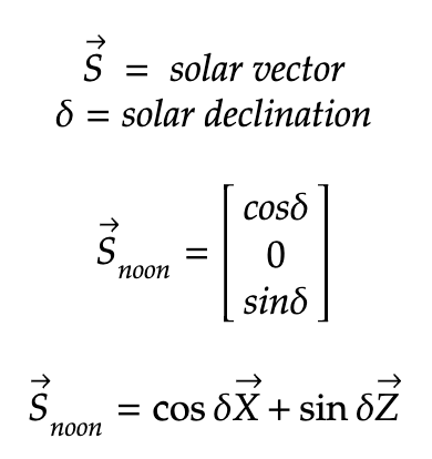
In other words, this vector is simply a unit direction tilted by an angle away from the equatorial plane, with no east–west component at noon.
The next step is to generalize this for any hour angle (H). The Sun is essentially sweeping across the sky, and in the equatorial frame, this motion is just a rotation around the Z-axis (Earth’s axis of rotation). So, rather than building a new vector, we just rotate the noon vector we derived earlier by H. The rotation matrix is:
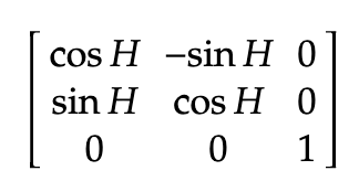
This rotation matrix is mixing the X and Y components using cos H and sin H, but leaves the Z component unchanged: [0, 0, 1]. I had to watch a few linear algebra videos on YouTube to understand rotation matrices and how they transform vectors. That’s beyond the scope of this blog post, though. We can now rotate our solar noon with this rotation matrix to understand how the hour angle affects it:
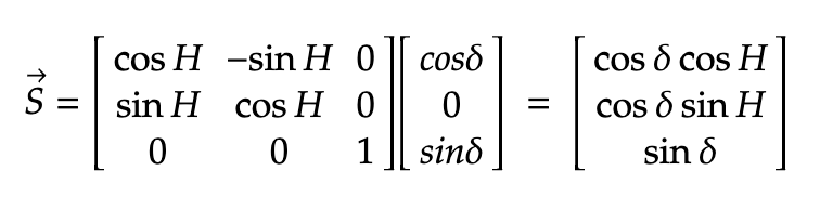
So, now we have a representation of the solar vector from the Earth’s frame of reference, which includes the declination and hour angle. Wonderful! Now, the last piece of the puzzle is to figure out how this vector looks from our local perspective using the ENU frame. This is where latitude finally comes into play.
To translate our solar vector into the ENU frame, we’d have to first define the ENU basis vectors in the equatorial frame. The East vector is the same as the Y-axis in the equatorial frame, so it would remain unchanged. The East and North vectors are essentially the X and Y basis vectors (in the equatorial frame) rotated by our latitude. To visualize this, imagine looking down from the Y-basis vector and rotating the X and Z vectors by the latitude (𝜙):
We can now define the ENU vectors in topocentric equatorial space:
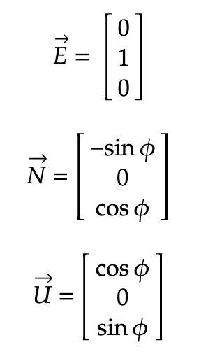
The E component is unchanged: [0, 1, 0]. N and U are rotated by the latitude. We can make these vectors the columns of a matrix and get the ENU basis matrix:
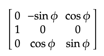
The first column corresponds to East (E), the second to North (N), and the third to Up (U). This matrix encodes the observer’s latitude and defines how the global (equatorial) frame is oriented relative to the local one. The next step is to project the solar vector we obtained earlier (defined in the equatorial frame) in this local coordinate system. We do this by multiplying it with the ENU basis matrix, which effectively projects the Sun’s direction onto the East, North, and Up axes. In other words, this tells us what the Sun’s direction looks like from our local perspective:
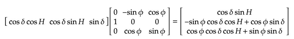
So, now we have a representation of the solar vector that contains everything we need: hour angle, solar declination, and latitude. Excellent! The top row represents the “E” component of the solar vector, the next one represents the “N” component, and the last one represents the “U” component.
Altitude and Azimuth
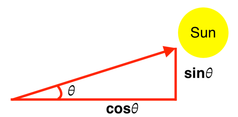
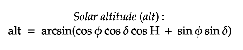
The solar altitude is the angle between the local horizon and the sun.
The vertical component here also equals the solar “U” component in the ENU frame. So, the altitude is:
The azimuth is the angle between the “E” and “N” components:
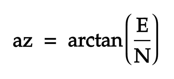
This needs to be corrected based on the signs of E and N so that it lies in the correct direction:
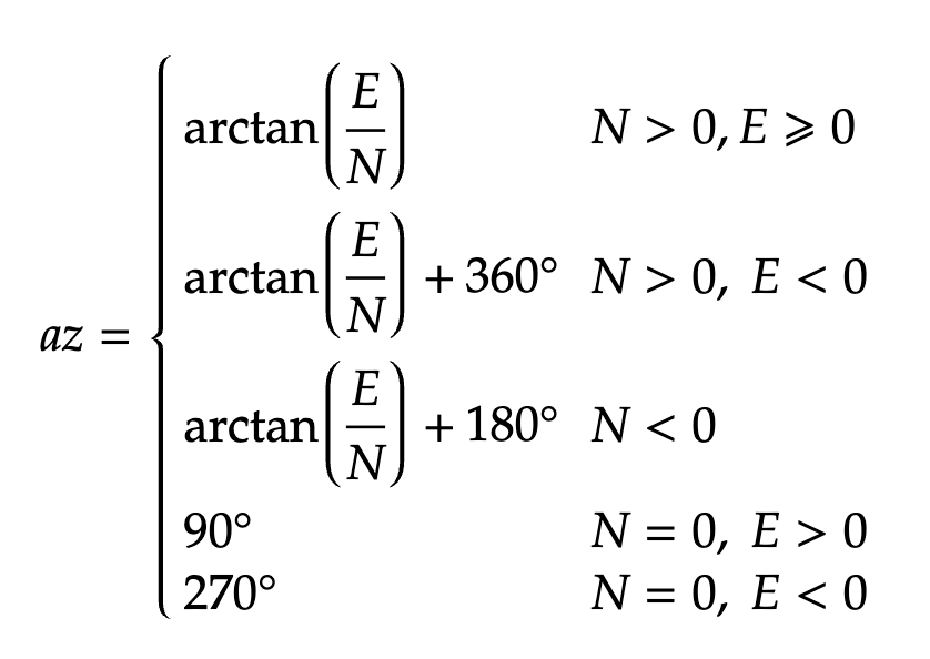
These cases are the equivalent of using the atan2 function in languages such as Python.
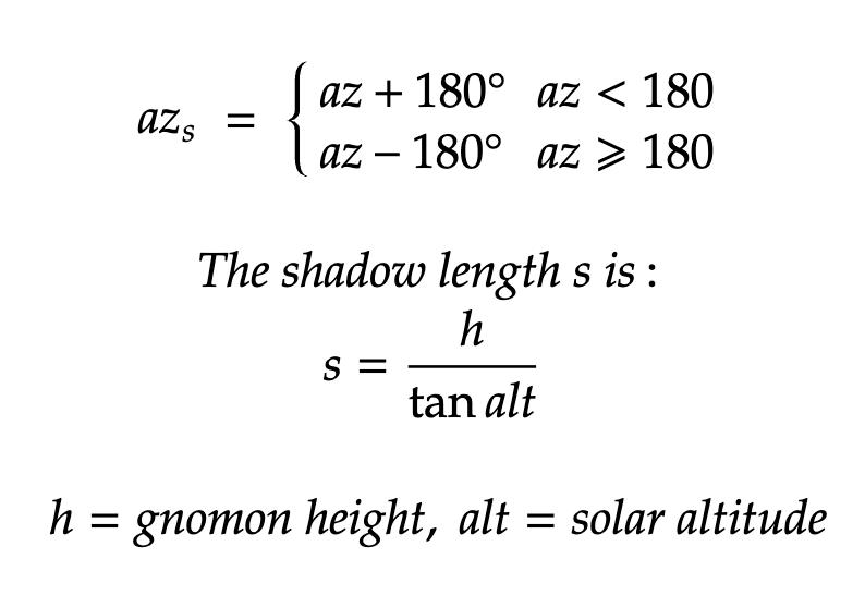
Once we know the altitude and azimuth, we can determine the length and direction of the shadow using trigonometry. A shadow always points directly opposite the Sun, so its azimuth is simply reversed. The shadow’s direction and length can therefore be expressed as:
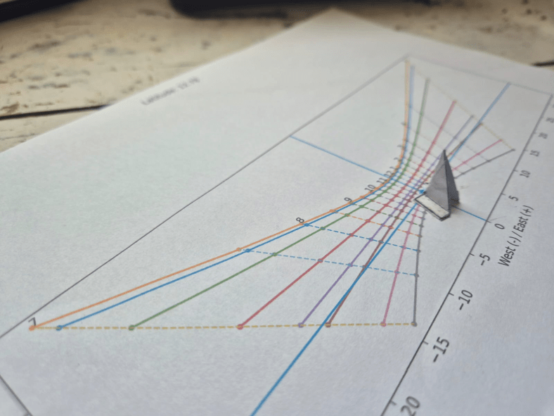
To test the equations, I calculated where the shadow of a 4cm gnomon should fall on a piece of paper at a specific time. Seeing the shadow tip land exactly where the math predicted was really exciting! I later wrote a Python script to generate lines for different months. My Python scripts are in this GitHub repository.
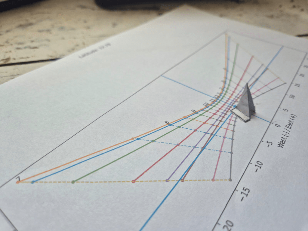
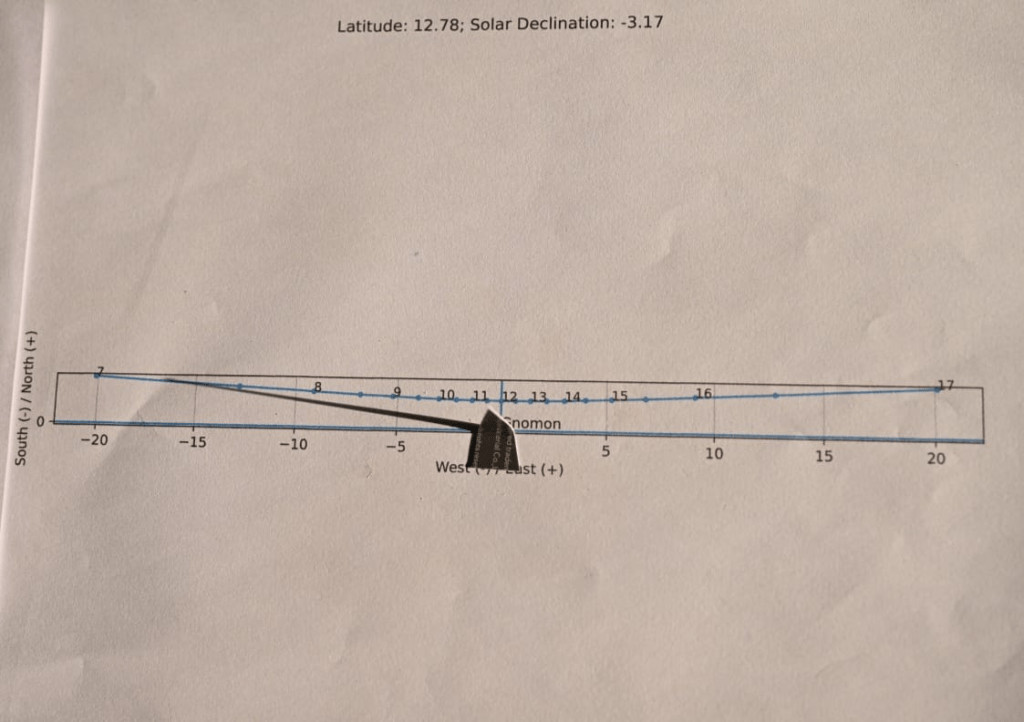
One interesting result is that the line corresponding to the March and September equinoxes becomes a perfectly straight line, whereas the lines for the other months produce curves. Why does this happen? There are a few ways to explain this. An intuitive explanation is that the shadow is a two-dimensional projection of a three-dimensional motion (the Sun’s path across the sky). Only under special conditions does that projection reduce to a straight line. Another explanation comes from the mathematics itself, where the equations simplify in a way that removes the curvature entirely. I’ll leave that as an exercise for you to explore!