I have been working on a QRP CW transmitter which I’ve described in an earlier post. The output from the buffer amplifier stage is about 50 mW. My goal is to reach about 5 watts of power. To do so, I plan to use the ubiquitous IRF510 transistor to boost power levels. The IRF510 MOSFET is a type of field-effect transistor. It was developed in the 1970s by a semiconductor manufacturing company – International Rectifier. It was originally intended to be used in the automotive industry for turn-signal blinkers and headlight dimmers to replace clunky electromechanical switches and relays. It still continues to be quite popular (and cheap). It has found its way into the hands of amateur radio experimenters who use it at frequencies way beyond what this humble transistor was intended for!
The final power amplifier in my transmitter would be a class-C amplifier using the IRF510. Before connecting the IRF510 to my circuit, I decided to investigate its input characteristics. This would help me to decide how to drive it and meet my design goals. MOSFETs typically have a very high input impedance in DC circuits since the gate is electrically insulated. However, in AC circuits, things are a little more complicated.
MOSFET basics
The IRF510 is an N-channel enhancement mode MOSFET. A MOSFET consists of an insulated gate, the voltage of which determines the conductivity of the device. The ability to regulate the flow of electricity with the amount of applied voltage can be used for amplifying or switching electrical signals.

A thin oxide layer insulates the gate from the rest of the transistor body. When a positive voltage is applied at the gate, positively charged holes are pushed away from the gate-insulator/semiconductor interface creating a depletion layer. The depletion layer is filled with negative charge carriers. With sufficient gate voltage, the accumulation of electrons forms a conducting path between the source and drain terminals, enabling current flow. The width and conductivity of the channel can be modulated by the voltage applied to the gate. The threshold voltage, commonly abbreviated as Vth of a field-effect transistor (FET) is the minimum gate-to-source voltage (Vgs) that is needed to create a conducting path between the source and drain terminals.
Gate capacitance
The gate of the MOSFET is electrically insulated because of the oxide layer, which gives it a high input impedance. When a DC voltage is applied to the gate, no current flows through the gate. The insulating oxide layer is sandwiched between two conductive layers. However, whenever two conductors are separated by an insulating layer, there will be some capacitance. Oftentimes this parasitic capacitance is an unwanted side effect. In the case of MOSFETs, this implies that the gate won’t appear high impedance to an AC input signal since capacitors allow AC signals.
The transistor datasheet should mention the gate capacitance. For the IRF510, the datasheet states a gate capacitance of about 180 pF. This could also be measured in several ways.
Observing the depletion layer
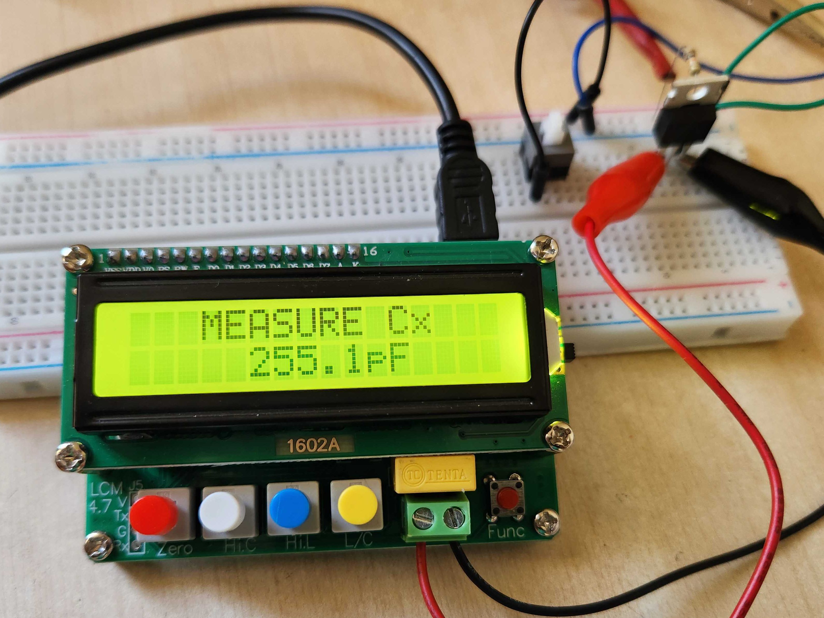
We can measure the capacitance between the gate and source pins using an LCR meter. When measuring the capacitance, I noticed that this capacitance decreases when voltage is applied to the drain and source pins (Vds). I guess this is because of the formation of the depletion layer. As the depletion layer widens, the capacitance decreases.

Analysis with a signal generator and oscilloscope
Gate capacitance could also be determined using AC analysis with a signal generator and oscilloscope. This method involves some math.
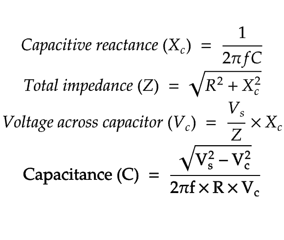
We connect a known resistor (R) in series with the gate to create a series RC circuit. Vs is the peak-to-peak from the signal generator, and Vc is the peak-to-peak voltage measured across the capacitor on the scope. The first equation is the formula for capacitive reactance since a capacitor behaves as a frequency-dependent resistor in an AC circuit. The second equation calculates the total impedance by taking the Pythagorean sum of R and Xc. You can read more about impedance in RLC circuits here. The third equation is Ohm’s law: V = IR. The voltage across the capacitor (Vc) is equal to the total current (Vs / Z) multiplied by the reactance of the capacitor (Xc). I derived the formula for capacitance from the first three equations. If you use this method, make sure you consider the output impedance of the signal generator in your calculations.
An interesting phenomenon
While trying to determine the gate capacitance, I tried measuring the RC time constant by charging the gate capacitor through a known resistor. The RC time constant equals R x C (R is in ohms, C is in farads). The time constant is the time it takes for a capacitor to acquire 63.2% of the difference between its initial voltage charge and the voltage applied to it. When I tried measuring this, I noticed something unusual.
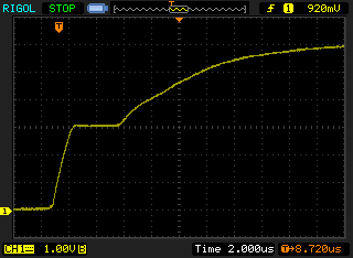
The graph doesn’t look like a typical capacitor charge graph. There is a region where it plateaus for a while before it resumes charging again.
This effect was first discovered in the 1920s by John Milton Miler when working with triode vacuum tube amplifiers. The parasitic capacitance between the grid and anode affected the performance of the triode amplifier. This effect is called “Miller effect”. According to Wikipedia:
“In electronics, the Miller effect accounts for the increase in the equivalent input capacitance of an inverting voltage amplifier due to amplification of the effect of capacitance between the input and output terminals.“
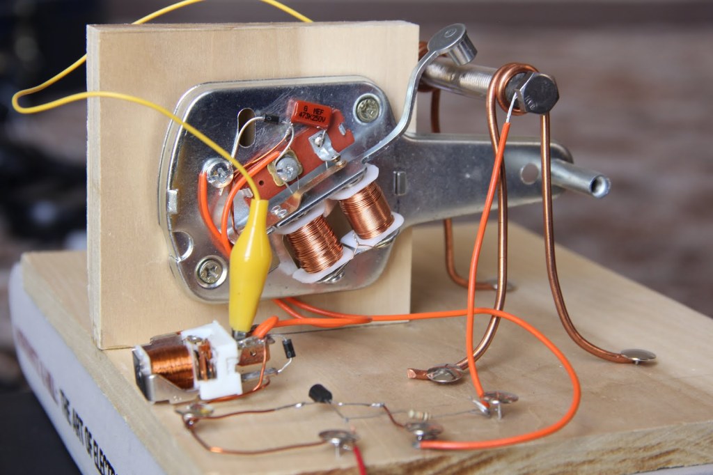
Later on, we invented solid-state transistors that replaced vacuum tubes, but the Miller effect didn’t go away. There’s no getting around physics! To observe the Miller effect on a scope, I added a 10K resistor in series with the MOSFET’s gate. This resistor slows the charging time of the parasitic capacitors and allows us to see the Miller effect in all its glory.
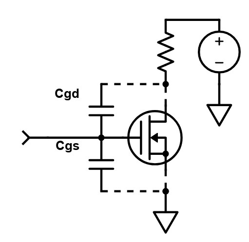
In a MOSFET, there is parasitic capacitance between the gate and source (Cgs) and between the gate and drain (Cgd). There is also parasitic capacitance between the drain and the source, but we will ignore that for now. Initially, when there is no voltage at the gate, the Cgs capacitor is at 0V. The Cgd capacitor is charged to the supply voltage since the voltage at the drain is whatever the supply voltage is.
When the gate voltage rises, the Cgs capacitor charges until the MOSFET’s Vth threshold is reached. This is the voltage at which a channel is formed between the drain and the source. As the MOSFET switches on, the drain voltage drops, and eventually approaches the source voltage. When it drops, the Cgd capacitor sucks in current from the gate, preventing its voltage from rising. This is why we see the plateau in the graph. When the drain voltage settles, and the Cgd capacitor is fully saturated, the gate voltage continues rising.
How do we counter this effect? Of course, the higher the input drive current, the quicker it would pass the Miller plateau. There are other more complicated techniques to counter this effect. I don’t fully understand them yet.
The reality is that I can’t just drive the IRF510 with the 50 mW output from the buffer amplifier and expect 5 watts of output power. According to “Handiman’s guide to MOSFET amplifiers”, the input impedance is about 130 ohms at 7 MHz (40-meter band). To provide an 8 Vpp at that impedance, we’d require about a half-watt of drive. I would have to add another amplifier stage to drive the IRF510.